
- ASIC
- 电池管理IC与BMS解决方案
- 时钟和时序解决方案
- ESD 和浪涌保护器件
- 汽车以太网
- 评估板
- 高可靠性
- 隔离
- 存储器
- 微控制器
- 功率产品
- 射频
- 安全智能卡解决方案
- 传感器技术
- 小信号晶体管和二极管
- 收发器
- 通用串行总线(USB)
- 无线连接
- 英飞凌大中华区生态圈
- 搜索工具
- 技术
- 封装
- 订单
- 概览
- 嵌入式闪存eFlash IP 解决方案
- RAM和Flash多芯片封装MCP解决方案
- F-RAM铁电存储器
- NOR 闪存
- nvsRAM非易失性存储器
- PSRAM — 伪静态RAM
- 抗辐射和高可靠性的存储器
- SRAM静态随机存储器
- 晶圆和裸片存储器解决方案
- 概览
- Calypso® 产品
- CIPURSE™ 产品
- 非接触式存储
- 了解 OPTIGA™ 嵌入式加密解决方案
- SECORA™ 安全解决方案
- 安全控制器
- 智能卡模块
- 政府身份证的智能解决方案
- 概览
- REAL3™ 3D ToF 图像传感器
- 电流传感器
- 气体传感器
- Inductive position sensors
- 微机电系统麦克风
- 压力传感器
- 雷达传感器
- 磁性位置传感器
- 磁性速度传感器
- Capacitive sensors
- Temperature sensors
- Battery sensors
- Digital X-ray
- Computed tomography
- Sensor interface ASICs
- 概览
- USB 2.0 外设控制器
- USB 3.2 外设控制器
- USB 集线器控制器
- USB PD 高压微控制器
- USB-C AC-DC 和 DC-DC 充电解决方案
- USB-C 充电端口控制器
- USB-C 供电控制器
- 概览
- AIROC™ 车载无线
- AIROC™ 蓝牙Bluetooth® 和多协议解决方案
- AIROC™ 互联微控制器
- AIROC™ Wi-Fi + Bluetooth® 组合
- AIROC™ Ultra-Wide Band Solutions
- 概览
-
TriCore™ AURIX™ TC2x安全模块
- 概览
- AURIX™系列 – TC21xL
- AURIX™ 系列 – TC21xSC (无线充电)
- AURIX™ 系列 – TC22xL
- AURIX™系列 – TC23xL
- AURIX™ 系列 – TC23xLA (ADAS)
- AURIX™ 系列 – TC23xLX
- AURIX™ 系列 – TC264DA (ADAS)
- AURIX™系列 – TC26xD
- AURIX™ 系列 – TC27xT
- AURIX™ 系列 – TC297TA (ADAS)
- AURIX™ 系列 – TC29xT
- AURIX™ 系列 – TC29xTT (ADAS)
- AURIX™系列 – TC29xTX
- AURIX™ TC2x仿真器件
- 32 位TriCore™ AURIX™ – TC3x
- 32 位TriCore™ AURIX™ - TC4x
- 概览
- PSOC™ 4 Arm® Cortex® -M0/M0+
- PSOC™ 4 HV Arm® Cortex® -M0+
- PSOC™ 5 LP Arm® Cortex® -M3
- PSOC™ 6 Arm® Cortex-M4®/M0+
- PSOC™ 多点触控触摸屏控制器
- PSOC™ Control C3 Arm® Cortex®-M33
- PSOC™ Automotive 4: Arm® Cortex®-M0/M0+
- PSOC™ Edge Arm® Cortex® M55/M33
- PSOC™ Control C1 Arm® Cortex®-M0
- 概览
- 32 位 TRAVEO™ T2G Arm® Cortex®用于车身电子应用
- 用于仪表盘的 32 位 TRAVEO™ T2G Arm® Cortex®
- 概览
- 桥式整流器和交流开关
- CoolSiC™ 肖特基二极管
- 二极管裸片
- 硅二极管
- 晶闸管/二极管模块
- 晶闸管软启动器模块
- 晶闸管/二极管盘
- 概览
- 汽车栅极驱动器
- 用于 GaN HEMT 的栅极驱动器 IC
- Gate Driver ICs for SiC MOSFETs
- Half-Bridge Gate Driver ICs
- High-Side Gate Driver ICs
- 电气隔离栅极驱动器
- 电平转换
- Low-Side Gate Driver ICs
- Three-Phase Gate Driver ICs
- 变压器驱动IC
- 概览
- BLDC 电机驱动器
- BDC电机驱动器
- 步进电机和伺服电机驱动器
- 带MCU的电机驱动器
- 使用 MOSFET 的桥式驱动器
- GaN EiceDRIVER™高速栅极驱动器
- 概览
- 车规级 MOSFET 30 V - 800 V
- 双 MOSFET
- MOSFET(Si 和 SiC)模块
- N 沟道耗尽型 MOSFET
- N 沟道 MOSFET
- P 沟道 MOSFET
- 碳化硅 CoolSiC™ MOSFET
- 250V至600V G14小信号MOS
- 概览
- OPTIGA™ Authenticate
- OPTIGA™ Authenticate NFC 解决方案
- OPTIGA™ Connect – 交钥匙式 eSIM 安全解决方案
- OPTIGA™ Trust
- OPTIGA™ 可信平台模块 (TPM)
- 概览
- EZ-PD™ ACG1F 单端口 USB-C 控制器
- EZ-PD™ CCG2 USB Type-C 端口控制器
- EZ-PD™ CCG3PA Automotive USB-C 和 Power Delivery 控制器
- EZ-PD™ CCG4 双端口 USB-C 和 PD
- EZ-PD™ CCG5 双端口和 CCG5C 单端口 USB-C PD 控制器
- EZ-PD™ CCG6 单端口 USB-C & PD 控制器
- EZ-PD ™ CCG6_CFP 和 EZ-PD ™ CCG8_CFP 双单端口 USB-C PD
- EZ-PD™ CCG6DF 双端口和 CCG6SF 单端口 USB-C PD 控制器
- EZ-PD™ CCG7D 汽车双口 USB-C PD + DC-DC 控制器
- EZ-PD™ CCG7S 汽车单口 USB-C PD 解决方案,配备DC-DC控制器
- EZ-PD™ CCG8 双/单口 USB-C PD
- EZ-PD™ CMG1 USB-C EMCA 控制器
- 支持 EPR 的 EZ-PD™ CMG2 USB-C EMCA 控制器
- 最新动态
- 航空航天
- 人工智能和数据中心
- 智能汽车解决方案
- 通讯
- 消费类电子产品
- 健康和 生活方式
- 工业
- 安全解决方案
- 智能家居和楼宇
- 解决方案
- 概览
- 电源适配器和充电器
- AR and smart glasses
- 光伏
- 无人机
- 家庭娱乐应用的半导体解决方案
- 家用电器
- 移动设备和智能手机解决方案
- 适用于智能电视的完整系统解决方案
- 智能会议系统
- 消费类可穿戴设备
- 概览
- 资产跟踪
- 电池化成和测试
- 电源适配器和充电器
- 工业机器人
- 轻型电动车解决方案
- 不间断电源 (UPS)
- Digital health
- 电动叉车
- Battery energy storage (BESS)
- 电动汽车充电
- 高压固态配电系统
- 氢电解
- 工业自动化
- 工业电机驱动和控制
- 工业& 医疗 SMPS
- LED 照明系统设计
- 光伏
- 电动工具
- 电力传输和配电
- 机器人
- 轨交
- Wind power
- 最新动态
- 概览
- AIROC™ 软件&工具
- AURIX™应用软件
- DRIVECORE™ 用于汽车软件开发
- iMOTION™ 工具和软件
- Infineon智能功率开关和栅极驱动器工具套件
- MOTIX 软件&工具
- OPTIGA™工具和软件
- PSOC™ 软件&工具
- TRAVEO™ 软件&工具
- XENSIV™ 工具和软件
- XMC™ 工具和软件
- 概览
- EZ-PD™ CCGx Dock 软件开发工具包
- FMx Softune IDE
- Infineon GUI Designer
- ModusToolbox™ 软件
- PSOC™ Creator软件
- 雷达开发套件
- 锈
- USB 集线器控制器
- 无线连接蓝牙网状网络辅助应用程序
- XMC™ DAVE™ 软件
- 最新动态
- 支持
- 培训
- 英飞凌开发者社区
- 最新消息
商业财经新闻
16/09/2026
商业财经新闻
11/09/2026
商业财经新闻
09/09/2026
商业财经新闻
28/08/2026
- 公司名称
- 我们的故事
- 活动资讯
- 新闻中心
- 投资者
- 职业生涯
- 质量
- 最新消息
商业财经新闻
16/09/2026
商业财经新闻
11/09/2026
商业财经新闻
09/09/2026
商业财经新闻
28/08/2026
- 您即将进入英飞凌境外官方网站 Infineon.com。您的相关个人信息可能在境外被收集和处理, 用于交易、支付、履约及售后事宜
- 本境内网站 Infineon.cn 仅提供产品信息展示服务,不开展线上交易、订单处理、支付结算及电子商务平台运营活动
- 所有交易、支付、履约及售后事宜均由境外主体独立完成并承担全部法律责任
- 本网站与境外网站为独立运营主体,交易行为仅发生于您与境外运营主体之间
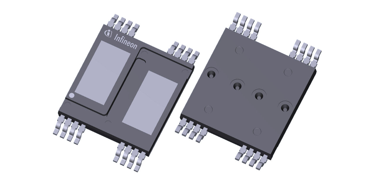
商品详情
-
Ciss1010 pF
-
Coss41 pF
-
最高 Ptot365 week
-
Qgd6.9 nC
-
QG28 nC
-
RDS (on) (@ Tj = 25°C)52.6 mΩ
-
最高 RthJA62 K/W
-
最高 RthJC0.64 K/W
-
最高 Tj175 °C
-
最高 VDS1200 V
-
安装SMD
-
封装PG-HDSOP-16-U03
-
工作温度 范围-55 °C 至 175 °C
-
引脚数量16 Pins
-
技术CoolSiC™ G2, CoolSiC™ G5
-
质量等级Industrial
| 推荐的 | |
|
OPN
|
IMSQ120R053M2HBXUMA1 |
| 产品状态 | active and preferred |
| 英飞凌封装名称 | |
| 封装名 | N/A |
| 封装尺寸 | 750 |
| 封装类型 | TAPE & REEL |
| 湿度 | 2 |
| 防潮封装 | DRY |
| 无铅 | Yes |
| 无卤素 | Yes |
| 符合RoHS标准 | Yes |
| 封装产地 |
MY
|
| 晶圆产地 |
AT,MY
|
|
|
|
| 产品状态 |
Active
|
|---|---|
| 英飞凌封装名称 | |
| 封装名 | - |
| 封装尺寸 | 750 |
| 封装类型 | TAPE & REEL |
| 湿度 | 2 |
| 防潮封装 | DRY |
| 无铅 | |
| 无卤素 | |
| 符合 RoHS 标准 | |
| 封装产地 |
MY
|
| 晶圆产地 |
AT,MY
|
特性
- VDSS = 1200 V at Tvj = 25°C
- IDDC = 31 A at TC = 25°C
- RDS = 52.6 mΩ, VGS = 18 V, Tvj = 25°C
- IF = 20 A
- Optimized layout for fast switching
- Very low switching losses
- No reverse recovery current
- High surge-current Schottky diode
- Short circuit withstand time 2 µs
- Best-in-class VGS(th): 4.2 V
- .XT interconnection technology
产品优势
- Higher power density
- Enabling automated assembly
- Less complex designs needed
- Outstanding thermal performance vs BSC
- Improve system power losses
- Enable a VRMS of 950 V with PD 2
- Lower BOM cost
微信分享
用微信扫描二维码并分享