- ASIC
- 电池管理 IC
- 时钟和时序解决方案
- ESD 和浪涌保护器件
- 汽车以太网
- 评估板
- 高可靠性
- 隔离
- 存储器
- 微控制器
- 功率产品
- 射频
- 安全智能卡解决方案
- 传感器技术
- 小信号晶体管和二极管
- 收发器
- 通用串行总线(USB)
- 无线连接
- 英飞凌大中华区生态圈
- 搜索工具
- 技术
- 封装
- 订单
- 概览
- 嵌入式闪存eFlash IP 解决方案
- RAM和Flash多芯片封装MCP解决方案
- F-RAM铁电存储器
- NOR 闪存
- nvsRAM非易失性存储器
- PSRAM伪静态随机存储器
- 抗辐射和高可靠性的存储器
- SRAM静态随机存储器
- 晶圆和裸片存储器解决方案
- 概览
- AC-DC电源转换
- 电动汽车动力系统
- D 类音频放大器 IC
- 非接触式电源和检测 IC
- DC-DC 转换器
- 二极管&晶闸管 (Si/SiC)
- 氮化镓(GaN)
- GaN EiceDRIVER™高速栅极驱动器
- IGBT 产品及驱动器件
- 智能功率模块(IPM)
- LED 驱动芯片
- 电动机驱动器
- MOSFETs
- 功率模块
- 电源模块
- 保护和监控IC
- 碳化硅 (SiC)
- 智能电源开关
- 固态继电器
- 无线充电 IC
- 概览
- Calypso® 产品
- CIPURSE™ 产品
- 非接触式存储
- 了解 OPTIGA™ 嵌入式加密解决方案
- SECORA™ 安全解决方案
- 安全控制器
- 智能卡模块
- 政府身份证的智能解决方案
- 概览
- USB 2.0 外设控制器
- USB 3.2 外设控制器
- USB 集线器控制器
- USB PD 高压微控制器
- USB-C AC-DC 和 DC-DC 充电解决方案
- USB-C 充电端口控制器
- USB-C 供电控制器
- 概览
- AIROC™ 车载无线
- AIROC™ 蓝牙Bluetooth® 和多协议解决方案
- AIROC™ 互联微控制器
- AIROC™ Wi-Fi + Bluetooth® 组合
- 概览
- FM0+ 32 位 Arm® Cortex-M0®+ 微控制器 (MCU) 系列
-
FM3 32 位 Arm® Cortex-M3® 微控制器 (MCU) 系列
- 概览
- FM3 CY9AFx1xK 系列 Arm® Cortex-M3® 微控制器 (MCU)
- FM3 CY9AFx1xL/M/N 系列 Arm® Cortex-M3® 微控制器 (MCU)
- FM3 CY9AFx2xK/L 系列 Arm® Cortex-M3® 微控制器 (MCU)
- FM3 CY9AFx3xK/L 系列超低漏电流 Arm® Cortex-M3® 微控制器 (MCU)
- FM3 CY9AFx4xL/M/N 系列低功耗 Arm® Cortex-M3® 微控制器 (MCU)
- FM3 CY9AFx5xM/N/R 系列低功耗 Arm® Cortex-M3® 微控制器 (MCU)
- FM3 CY9AFxAxL/M/N 系列超低漏电流 Arm® Cortex-M3® 微控制器 (MCU)
- FM3 CY9BFx1xN/R 高性能系列 Arm® Cortex-M3® 微控制器 (MCU)
- FM3 CY9BFx1xS/T 高性能系列 Arm® Cortex-M3® 微控制器 (MCU)
- FM3 CY9BFx2xJ 系列 Arm® Cortex-M3®微控制器 (MCU)
- FM3 CY9BFx2xK/L/M 系列 Arm® Cortex-M3® 微控制器 (MCU)
- FM3 CY9BFx2xS/T 系列 Arm® Cortex-M3® 微控制器 (MCU)
- FM4 32 位 Arm® Cortex-M4® 微控制器 (MCU) 系列
- 概览
-
TriCore™ AURIX™ TC2x安全模块
- 概览
- AURIX™系列 – TC21xL
- AURIX™ 系列 – TC21xSC (无线充电)
- AURIX™ 系列 – TC22xL
- AURIX™系列 – TC23xL
- AURIX™ 系列 – TC23xLA (ADAS)
- AURIX™ 系列 – TC23xLX
- AURIX™ 系列 – TC264DA (ADAS)
- AURIX™系列 – TC26xD
- AURIX™ 系列 – TC27xT
- AURIX™ 系列 – TC297TA (ADAS)
- AURIX™ 系列 – TC29xT
- AURIX™ 系列 – TC29xTT (ADAS)
- AURIX™系列 – TC29xTX
- AURIX™ TC2x仿真器件
- 32 位TriCore™ AURIX™ – TC3x
- 32 位TriCore™ AURIX™ - TC4x
- 概览
- PSOC™ 4 Arm® Cortex® -M0/M0+
- PSOC™ 4 HV Arm® Cortex® -M0+
- PSOC™ 5 LP Arm® Cortex® -M3
- PSOC™ 6 Arm® Cortex-M4®/M0+
- PSOC™ 多点触控触摸屏控制器
- PSOC™ Control C3 Arm® Cortex®-M33
- PSOC™ Automotive 4: Arm® Cortex®-M0/M0+
- PSOC™ Edge Arm® Cortex® M55/M33
- 概览
- 32 位 TRAVEO™ T2G Arm® Cortex®用于车身电子应用
- 用于仪表盘的 32 位 TRAVEO™ T2G Arm® Cortex®
- 概览
- 32 位XMC1000工业微控制器 Arm® Cortex-M0®
- 32 位XMC4000工业微控制器 Arm® Cortex-M4®
- XMC5000 Industrial Microcontroller Arm® Cortex®-M4F
- 32 位XMC7000工业微控制器 Arm® Cortex-M7®
- 概览
- 桥式整流器和交流开关
- CoolSiC™ 肖特基二极管
- 二极管裸片
- 硅二极管
- 晶闸管/二极管模块
- 晶闸管软启动器模块
- 晶闸管/二极管盘
- 概览
- PSOC™ Control C3 Arm® Cortex®-M33
- 电机控制系统级芯片 / 系统级封装
- BLDC 电机驱动器
- BDC电机驱动器
- 步进电机和伺服电机驱动器
- 带MCU的电机驱动器
- 使用 MOSFET 的桥式驱动器
- GaN EiceDRIVER™高速栅极驱动器
- 概览
- 汽车级MOSFET
- 双 MOSFET
- MOSFET(Si 和 SiC)模块
- N 沟道耗尽型 MOSFET
- N 沟道 MOSFET
- P 沟道 MOSFET
- 碳化硅 CoolSiC™ MOSFET
- 250V至600V G14小信号MOS
- 概览
- IGBT 模块
- MOSFET(Si 和 SiC)模块
- 智能功率模块(IPM)
- 二极管&晶闸管 (Si/SiC)
- IGBT CoolSiC™汽车功率模块
- 高密度功率模块
- 概览
- OPTIGA™ Authenticate
- OPTIGA™ Authenticate NFC 解决方案
- OPTIGA™ Connect – 交钥匙式 eSIM 安全解决方案
- OPTIGA™ Trust
- OPTIGA™ 可信平台模块 (TPM)
- 概览
- EZ-PD™ ACG1F 单端口 USB-C 控制器
- EZ-PD™ CCG2 USB Type-C 端口控制器
- EZ-PD™ CCG3PA Automotive USB-C 和 Power Delivery 控制器
- EZ-PD™ CCG4 双端口 USB-C 和 PD
- EZ-PD™ CCG5 双端口和 CCG5C 单端口 USB-C PD 控制器
- EZ-PD™ CCG6 单端口 USB-C & PD 控制器
- EZ-PD ™ CCG6_CFP 和 EZ-PD ™ CCG8_CFP 双单端口 USB-C PD
- EZ-PD™ CCG6DF 双端口和 CCG6SF 单端口 USB-C PD 控制器
- EZ-PD™ CCG7D 汽车双口 USB-C PD + DC-DC 控制器
- EZ-PD™ CCG7S 汽车单口 USB-C PD 解决方案,配备DC-DC控制器
- EZ-PD™ CCG7SAF 车规级单端口 USB-C PD + DC-DC 控制器 + FETs
- EZ-PD™ CCG8 双/单口 USB-C PD
- EZ-PD™ CMG1 USB-C EMCA 控制器
- 支持 EPR 的 EZ-PD™ CMG2 USB-C EMCA 控制器
- 最新动态
- 航空航天
- 智能汽车解决方案
- 消费类电子产品
- 健康和 生活方式
- 家用电器
- 工业
- 信息和通信技术
- 可再生能源
- 机器人
- 安全解决方案
- 智能家居和楼宇
- 解决方案
- 概览
- 电源适配器和充电器
- 适用于智能电视的完整系统解决方案
- 移动设备和智能手机解决方案
- 多旋翼飞机和无人机
- 电动工具
- 家庭娱乐应用的半导体解决方案
- 智能会议系统
- 概览
- 电池化成和测试
- 电动汽车充电
- 氢气
- 光伏
- Wind power
- Solid-state circuit breaker (SSCB)
- Battery energy storage (BESS)
- 概览
- 汽车辅助系统
- 车载网关
- 汽车pds配电系统
- 车身控制模块 (BCM)
- 舒适便捷电子产品
- 区域 DC-DC 转换器 48 V-12 V
- 区域控制器
- 最新动态
- 概览
- AIROC™ 软件&工具
- AURIX™应用软件
- DRIVECORE 用于汽车软件开发
- iMOTION™ 工具和软件
- Infineon智能功率开关和栅极驱动器工具套件
- MOTIX 软件&工具
- OPTIGA™工具和软件
- PSOC™ 软件&工具
- TRAVEO™ 软件&工具
- XENSIV™ 工具和软件
- XMC™ 工具和软件
- 概览
- EZ-PD™ CCGx Dock 软件开发工具包
- FMx Softune IDE
- ModusToolbox™ 软件
- PSOC™ Creator软件
- 雷达开发套件
- 锈
- USB 集线器控制器
- 无线连接蓝牙网状网络辅助应用程序
- XMC™ DAVE™ 软件
- 最新动态
- 支持
- 培训
- 英飞凌开发者社区
- 最新消息
商业财经新闻
10/03/2026
商业财经新闻
05/03/2026
商业财经新闻
04/03/2026
商业财经新闻
16/02/2026
- 公司名称
- 我们的故事
- 活动资讯
- 新闻中心
- 投资者
- 职业生涯
- 质量
- 最新消息
商业财经新闻
10/03/2026
商业财经新闻
05/03/2026
商业财经新闻
04/03/2026
商业财经新闻
16/02/2026
简介
混合动力汽车/纯电动汽车的发展对功率电子提出了大量需求。目前,绝大多数功率电子都是基于硅材料。然而,硅材料的使用达到了极限,而碳化硅(SiC)的出现则提供了更多的可能性。SiC能大大解决硅材料在稳定性和成本方面带来的限制:SiC技术已成熟,可用于汽车。
正文
Electrification in automobiles is steadily on the rise. With it, comes the need for highly efficient power semiconductors for plug-in hybrid and all-electric vehicles (xEVs). The advantages of silicon carbide (SiC) over conventional silicon (Si) chips can not only be leveraged in industrial applications, but in cars too. SiC’s increased efficiency and power density allows for higher autonomy (and smaller batteries), reduced system size and weight, fast charging, and ultimately greater customer acceptance for e-mobility. Thanks to technological advances, SiC semiconductors’ penetration in xEV subsystems will increase over the next decade.
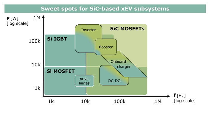
Currently power modules and discrete components typically use silicon-based diodes, MOSFETs, and IGBTs. By comparison, SiC circuits in xEV drivetrains enable smaller chip dimensions for the same power rating. In addition, the SiC technology reduces thermal losses. This means more efficient, lighter and more compact applications are now possible compared to previous systems. Typical applications that benefit from the advantages of SiC are main inverters, onboard charger electronics, boosters or DC/C converters (Figure 1).
Significant progress – SiC is ready for use in vehicles
For over two decades, SiC semiconductor components have been used in various applications. But there remained obstacles to be overcome before using them in automotive electronics. In order to be able to efficiently leverage the new technology in vehicles too, two main aspects had to be fulfilled: high reliability and cost-effectiveness.
In case of SIC MOSFET switches, the development of reliable gate-oxide has been a major road-block over many years. Recent breakthrough in the design (e.g. Trench concept) and manufacturing process has enabled devices meeting the reliability level requested by car manufacturers.
Moreover, SiC base material production (wafers) is significantly more complex resulting in smaller wafer diameters (Figure 2), higher number of defects per wafer, and higher cost. While Si crystal can be grown with high purity, the defect density in SiC wafers has been a major challenge. Significant progress has been made in recent years however, and defect density has been markedly reduced. Larger chip areas are finally possible, easing the integration into power packages.
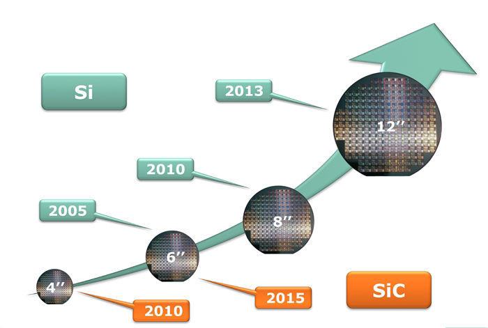
In the past, most SiC providers were small, specialized semiconductor manufacturers with relatively low volumes and little experience in the automotive industry. As a result, economies of scale were limited. But this situation has now fundamentally changed. The availability of high-quality 6-inch SiC wafers led to significant productivity improvements. The growth potential offered by the automotive market for SiC has become a compelling reason for leading semiconductor companies to enter this market. Current market reports confirm this trend.
Reducing losses by up to two thirds
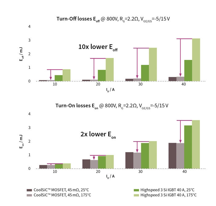
Compared to conventional silicon-based high-voltage IGBTs or MOSFETs (> 600V), SiC devices offer several advantages. For example, compared to IGBTs, SiC MOSFETs show no trail effect, almost no forward recovery nor reverse recovery. This results in temperature-independent switching losses that also are significantly lower than with silicon (Figure 3a). SiC Schottky diodes should also be noted in this context. High switching speeds or extremely low reverse recovery charges (Qrr) reduce the switching losses and make it possible to efficiently miniaturize the final product. SiC Schottky diodes are ideal for power factor correction (PFC) circuits in onboard charger systems.
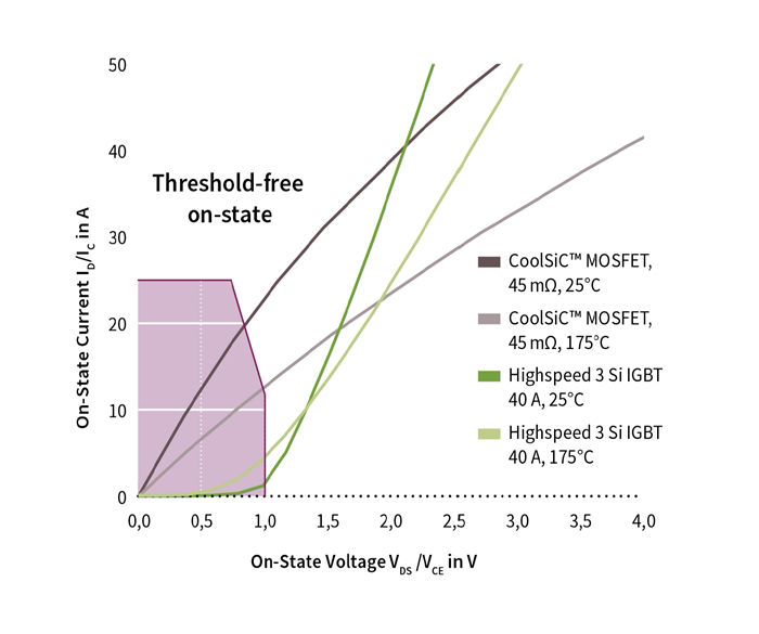
In addition to showing less switching losses, SiC MOSFETs have also advantages when it comes to conduction losses. Indeed, they exhibit a resistor-like output characteristic, compared to the diode-like characteristic of IGBTs. This threshold-free on-state characteristic results in smaller conduction losses in the partial load range (Figure 3b).
The basic advantages of SiC MOSFETs make them ideal for operation in onboard chargers or DC/DC converters where of smaller passive components can be used thanks to higher switching frequencies. They make them also ideal for inverter applications where switching frequencies lower than 20 kHz are typical. Here, the efficiency is substantially determined by the operation at partial load. SiC MOSFETs reduce the average thermal losses in inverters by up to two thirds.
Optimized packaging technology
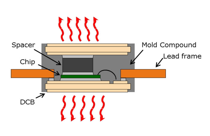
To make the most of the performance of the SiC chips, the power modules need a correspondingly optimized package technology. Higher power densities require not only improved packaging materials but also consideration for the higher thermal resistances of smaller chips leading to higher thermomechanical stress. Moreover, in order to be able to fully leverage the fast switching capability of the SiC MOSFETs, packages with low parasitic inductance are also required. This then calls for new packaging concepts for power modules. Modern packaging concepts with double-sided cooling are available to optimize thermal resistance of the devices. One example are the power modules HybridPACK™ DSC (double-sided cooling) from Infineon. They feature double-sided efficient heat dissipation and can thus significantly reduce the thermal resistance Rth at the system level (Figure 4). This makes it possible to build inverter designs with extremely high power density.
Significant cost reductions possible
SiC MOSFETs enable to realize very compact and highly efficient inverters. This is the conclusion of the Fraunhofer Institute for Integrated Systems and Component Technology (IISB) drew in its study “Evaluation of potentials for Infineon SiC MOSFETs in automotive inverter applications”. Under comparable conditions, the SiC MOSFETs significantly reduced the chip area compared to IGBT-based inverters. Thanks to the reduced chip losses, the efficiency for different driving scenarios has been improved by more than 3 percent, especially in city traffic with lots of acceleration phases.
When considering the inverter efficiency, it should be noted that the energy flows in two directions – from the battery to the wheel when generating the torque and back from the wheel to the battery during the energy recovery (recuperation). The efficiency of the inverter is thus essential for battery all-electric vehicles because it has a direct impact on the achievable range or the battery size needed to ensure a certain range. Since the battery is a key cost factor, a reduction of the battery cells by 5 to 10 percent can lead to a significant cost reduction in the system with batteries of more than 40 kWh output.
Silicon does not support high breakdown field strengths as efficiently as SiC does. A standard 1200 V IGBT has significantly greater losses than its counterpart in the 600 V class, whereas a 1200 V SiC MOSFET allows very efficient operation at higher battery voltages in the range of 850 V. This makes SiC particularly suitable for architectures that also enable fast-charging applications. With the charging station infrastructure currently under development, an 80 kWh battery will be charged to 80 percent in just 15 minutes. This means that one of the biggest obstacles to implementing electro-mobility will have been eliminated.
Conclusion
Although SiC material is more expensive than silicon, it allows to drastically increase power density. At a given power requirement, the semiconductor content can be reduced by factor 5. Infineon has manufactured its Trench-based SiC MOSFETs on 150 mm wafers right from the start. Considering the advantages at the system level – for example, more compact design, lower cooling effort, lighter systems, efficiency benefits – SiC is already competitive in its first applications.
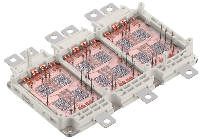
An increasing number of system manufacturers (Tier 1s) and car manufacturers (OEMs) are relying on SiC for future developments. With its 1200 V CoolSiC™ MOSFETs, Infineon intends to reach new efficiencies and performance levels. Studies based on the power module HybridPACK™ Drive CoolSiC (figure 5) have demonstrated the feasibility of having compact inverters providing more than 200 kW power at 850 V.
Infineon offers a broad portfolio of silicon and wideband gap semiconductors for power electronics, coupled with innovative packaging technology and gate drivers. Infineon has been developing for 25 years SiC solutions for photovoltaic inverters, windcrafts and industrial applications. Infineon is fully committed to introduce the advantages of SiC in the xEV world.